- 您现在的位置:买卖IC网 > Sheet目录3818 > PIC18F4620-I/ML (Microchip Technology)IC MCU FLASH 32KX16 44QFN
1996 Microchip Technology Inc.
DS30412C-page 81
PIC17C4X
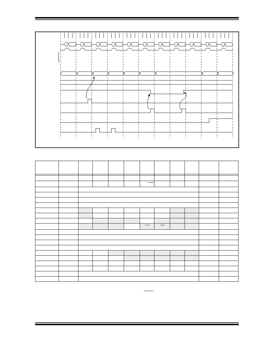
FIGURE 12-10: TMR1, TMR2, AND TMR3 OPERATION IN TIMER MODE
TABLE 12-6:
SUMMARY OF TMR1, TMR2, AND TMR3 REGISTERS
Address
Name
Bit 7
Bit 6
Bit 5
Bit 4
Bit 3
Bit 2
Bit 1
Bit 0
Value on
Power-on
Reset
Value on all
other resets
(Note1)
16h, Bank 3
TCON1
CA2ED1
CA2ED0
CA1ED1
CA1ED0
T16
TMR3CS TMR2CS TMR1CS 0000 0000
0000 0000
17h, Bank 3
TCON2
CA2OVF
CA1OVF PWM2ON PWM1ON CA1/PR3 TMR3ON TMR2ON TMR1ON 0000 0000
0000 0000
10h, Bank 2
TMR1
Timer1 register
xxxx xxxx
uuuu uuuu
11h, Bank 2
TMR2
Timer2 register
xxxx xxxx
uuuu uuuu
12h, Bank 2
TMR3L
TMR3 register; low byte
xxxx xxxx
uuuu uuuu
13h, Bank 2
TMR3H
TMR3 register; high byte
xxxx xxxx
uuuu uuuu
16h, Bank 1
PIR
RBIF
TMR3IF
TMR2IF
TMR1IF
CA2IF
CA1IF
TXIF
RCIF
0000 0010
17h, Bank 1
PIE
RBIE
TMR3IE
TMR2IE
TMR1IE
CA2IE
CA1IE
TXIE
RCIE
0000 0000
07h, Unbanked
INTSTA
PEIF
T0CKIF
T0IF
INTF
PEIE
T0CKIE
T0IE
INTE
0000 0000
06h, Unbanked
CPUSTA
—
STKAV
GLINTD
TO
PD
—
--11 11--
--11 qq--
14h, Bank 2
PR1
Timer1 period register
xxxx xxxx
uuuu uuuu
15h, Bank 2
PR2
Timer2 period register
xxxx xxxx
uuuu uuuu
16h, Bank 2
PR3L/CA1L
Timer3 period/capture1 register; low byte
xxxx xxxx
uuuu uuuu
17h, Bank 2
PR3H/CA1H Timer3 period/capture1 register; high byte
xxxx xxxx
uuuu uuuu
10h, Bank 3
PW1DCL
DC1
DC0
—
xx-- ----
uu-- ----
11h, Bank 3
PW2DCL
DC1
DC0
TM2PW2
—
xx0- ----
uu0- ----
12h, Bank 3
PW1DCH
DC9
DC8
DC7
DC6
DC5
DC4
DC3
DC2
xxxx xxxx
uuuu uuuu
13h, Bank 3
PW2DCH
DC9
DC8
DC7
DC6
DC5
DC4
DC3
DC2
xxxx xxxx
uuuu uuuu
14h, Bank 3
CA2L
Capture2 low byte
xxxx xxxx
uuuu uuuu
15h, Bank 3
CA2H
Capture2 high byte
xxxx xxxx
uuuu uuuu
Legend: x = unknown, u = unchanged, - = unimplemented read as '0', q - value depends on condition,
shaded cells are not used by TMR1, TMR2 or TMR3.
Note 1:
Other (non power-up) resets include: external reset through MCLR and WDT Timer Reset.
Q1Q2 Q3 Q4 Q1Q2 Q3 Q4 Q1Q2 Q3 Q4 Q1Q2 Q3 Q4 Q1Q2 Q3 Q4 Q1Q2 Q3 Q4 Q1Q2 Q3 Q4 Q1Q2 Q3 Q4 Q1Q2 Q3 Q4 Q1Q2 Q3 Q4 Q1Q2 Q3 Q4
AD15:AD0
ALE
Instruction
fetched
TMR1
PR1
TMR1ON
WR_TMR1
WR_TCON2
TMR1IF
RD_TMR1
TMR1
reads 03h
TMR1
reads 04h
MOVWF
TMR1
Write TMR1
MOVF
TMR1, W
Read TMR1
MOVF
TMR1, W
Read TMR1
BSF
TCON2, 0
Stop TMR1
BCF
TCON2, 0
Start TMR1
MOVLB
3
NOP
04h
05h
03h
04h
05h
06h
07h
08h
00h
发布紧急采购,3分钟左右您将得到回复。
相关PDF资料
PIC24HJ256GP210-I/PT
IC PIC MCU FLASH 128KX16 100TQFP
PIC24HJ128GP310A-I/PF
IC PIC MCU FLASH 128KB 100-TQFP
DSPIC33FJ128GP310-I/PF
IC DSPIC MCU/DSP 128K 100TQFP
PIC16C66-20I/SO
IC MCU OTP 8KX14 PWM 28SOIC
DSPIC33FJ128MC510-I/PT
IC DSPIC MCU/DSP 128K 100TQFP
PIC16C66-20I/SP
IC MCU OTP 8KX14 PWM 28DIP
PIC18LF2620-I/SP
IC MCU FLASH 32KX16 28SDIP
PIC16F877-04I/P
IC MCU FLASH 8KX14 EE 40DIP
相关代理商/技术参数
PIC18F4620-I/P
功能描述:8位微控制器 -MCU 64KB 3968 RAM 36 I/O RoHS:否 制造商:Silicon Labs 核心:8051 处理器系列:C8051F39x 数据总线宽度:8 bit 最大时钟频率:50 MHz 程序存储器大小:16 KB 数据 RAM 大小:1 KB 片上 ADC:Yes 工作电源电压:1.8 V to 3.6 V 工作温度范围:- 40 C to + 105 C 封装 / 箱体:QFN-20 安装风格:SMD/SMT
PIC18F4620-I/P
制造商:Microchip Technology Inc 功能描述:IC 8BIT FLASH MCU 18F4620 DIP40
PIC18F4620-I/PT
功能描述:8位微控制器 -MCU 64KB 3968 RAM 36 I/O RoHS:否 制造商:Silicon Labs 核心:8051 处理器系列:C8051F39x 数据总线宽度:8 bit 最大时钟频率:50 MHz 程序存储器大小:16 KB 数据 RAM 大小:1 KB 片上 ADC:Yes 工作电源电压:1.8 V to 3.6 V 工作温度范围:- 40 C to + 105 C 封装 / 箱体:QFN-20 安装风格:SMD/SMT
PIC18F4620-I/PT
制造商:Microchip Technology Inc 功能描述:IC 8BIT FLASH MCU 18F4620 TQFP44
PIC18F4620T-I/ML
功能描述:8位微控制器 -MCU 64KB 3968 RAM 36 I/O RoHS:否 制造商:Silicon Labs 核心:8051 处理器系列:C8051F39x 数据总线宽度:8 bit 最大时钟频率:50 MHz 程序存储器大小:16 KB 数据 RAM 大小:1 KB 片上 ADC:Yes 工作电源电压:1.8 V to 3.6 V 工作温度范围:- 40 C to + 105 C 封装 / 箱体:QFN-20 安装风格:SMD/SMT
PIC18F4620T-I/PT
功能描述:8位微控制器 -MCU 64KB 3968 RAM 36 I/O RoHS:否 制造商:Silicon Labs 核心:8051 处理器系列:C8051F39x 数据总线宽度:8 bit 最大时钟频率:50 MHz 程序存储器大小:16 KB 数据 RAM 大小:1 KB 片上 ADC:Yes 工作电源电压:1.8 V to 3.6 V 工作温度范围:- 40 C to + 105 C 封装 / 箱体:QFN-20 安装风格:SMD/SMT
PIC18F4680-E/ML
功能描述:8位微控制器 -MCU 64KB 3328 RAM w/ECAN RoHS:否 制造商:Silicon Labs 核心:8051 处理器系列:C8051F39x 数据总线宽度:8 bit 最大时钟频率:50 MHz 程序存储器大小:16 KB 数据 RAM 大小:1 KB 片上 ADC:Yes 工作电源电压:1.8 V to 3.6 V 工作温度范围:- 40 C to + 105 C 封装 / 箱体:QFN-20 安装风格:SMD/SMT
PIC18F4680-E/P
功能描述:8位微控制器 -MCU 64KB 3328 RAM w/ECAN RoHS:否 制造商:Silicon Labs 核心:8051 处理器系列:C8051F39x 数据总线宽度:8 bit 最大时钟频率:50 MHz 程序存储器大小:16 KB 数据 RAM 大小:1 KB 片上 ADC:Yes 工作电源电压:1.8 V to 3.6 V 工作温度范围:- 40 C to + 105 C 封装 / 箱体:QFN-20 安装风格:SMD/SMT